移相全桥DC-DC变换器的研究毕业论文
2020-04-15 20:16:41
摘 要
电力电子的相关产品被广泛应用于现实生活中,其发展速度十分迅猛,生活中到处可见其影子。与硬开关技术相比,软开关技术应用更广泛,更受到人们的青睐,能够方便简单的完成开关管的零电压开通(ZVS)。
DC-DC变换器不仅能够实现能量的转换,最重要的是它具有ZVS功能,本文目的之一即为根据对拓扑图的分析,研究其工作原理,找到要想实现滞后臂的ZVS需要有什么样的条件,从而设计出谐振器件的参数。本文对变换器的建模主要运用两种方法,其一:小信号建模法,其二:PWM等效法。
目的之二即为根据所建立的模型,设计PI控制器的参数,还介绍了变压器发生偏磁的原因,并对其进行偏磁补偿。
最后,通过Matlab/Simulink对系统进行仿真,验证建立的数学模型是否正确,以及PI控制器的参数的设计是否合理。
关键词:移相全桥DC-DC变换器 数学建模 PI控制器 偏磁 仿真
Research on Phase-Shifted Full-Bridge DC-DC Converter
Abstract
The related products of power electronics are widely used in real life. Their development speed is very fast, and their shadow can be seen everywhere in life.Compared with hard switching technology, soft switching technology is more widely used and more popular. It can easily and simply complete zero-voltage switching-on of switches(ZVS).
DC-DC converter can not only realize energy conversion, but also has ZVS function. One of the purposes of this paper is to study the working principle of DC-DC converter based on the analysis of the topology diagram and find out what conditions are needed to realize the ZVS of the lagging arm, so as to design the parameters of the resonant device.In this paper, two methods are used to model the converter. One is the small signal modeling method, the other is the PWM equivalent method.
The second purpose is to design the parameters of PI controller according to the established model, and introduce the cause of magnetic bias of transformer and compensate for it.
Finally, through the simulation software called Matlab/Simulink, the designed system is simulated to verify the correctness of the established mathematical model and the rationality of the PI controller parameter design.
Key words: phase-shifted full-bridge DC-DC converter; mathematical modeling; PI controller; magnetic bias; simulation
目 录
摘要 I
Abstract II
第一章 绪论 1
1.1研究背景及意义 1
1.2国内、外发展现状 1
1.2.1移相全桥DC-DC变换器的概述 1
1.2.2移相全桥DC-DC变换器的建模 4
1.2.3 变换器的偏磁问题 4
1.3研究内容 5
第二章 移相全桥DC-DC变换器的工作原理及参数设计 6
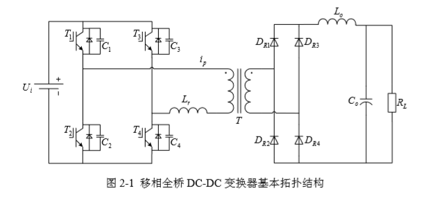
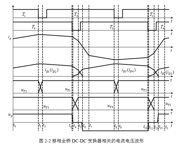
2.1 变换器的拓扑结构 6
2.2 变换器的工作原理 6
2.3主电路参数设计 12
2.3.1 高频变压器的参数设计 13
2.3.2 输出LC滤波器的参数设计 15
2.3.3 IGBT的选型 16
2.3.4 整流二极管的选择 17
第三章 移相全桥DC-DC变换器系统的建模与仿真 18
3.1 小信号模型建模 18
3.1.1 BUCK变换器的小信号模型 18
3.1.2 变换器的小信号模型 22
3.2 PWM等效建模法 24
3.3 控制器的设计 26
3.4 Matlab/Simulink系统仿真 28
第四章 高频变压器偏磁的检测与补偿 31
4.1 高频变压器偏磁的原因 31
4.2 高频变压器的偏磁检测 32
4.3 高频变压器偏磁补偿 34
第五章 实验结果 36
5.1 滞后臂ZVS的实现 36
5.2 稳态输出波形 37
5.3 偏磁补偿波形 38
第六章 总结与展望 40
参考文献 41
致谢 44
第一章 绪论
1.1研究背景及意义
近年来,电力电子的相关产品被广泛应用于现实生活中,其发展速度十分迅猛,生活中到处可见其影子,为了使电力电子产品效率更高,成本更低,且具有更高的可靠性,软开关技术越来越受到青睐,成为了新的发展趋势[1]。
虽然高频化能减小功率变压器的体积及成本,可是,因为遭到功率开关管通断速率的限定,会增加其损耗;虽然软开关技术能减小电磁干扰及通断损耗,可是通常情况下需要额外增加电路,从而使系统复杂化;数字控制器采用数字芯片,具有控制灵活、可靠性高的特点,受到广泛应用[1]。
1.2国内、外发展现状
1.2.1移相全桥DC-DC变换器的概述
移相全桥DC-DC变换器一般采取PWM控制的方法,功率开关管具有四种不同的状态,整体上可分为暂态和稳态。
如图1-1所示,硬开关时,在过度过程中,功率开关管的损耗较大,所以在高频场合中一般不运用硬开关技术。因回路中设有寄生电感和电容,所以在通断过程中,系统的电磁干扰会增大[2]。
以上是毕业论文大纲或资料介绍,该课题完整毕业论文、开题报告、任务书、程序设计、图纸设计等资料请添加微信获取,微信号:bysjorg。
相关图片展示: