面向自动光学检测系统的路径规划设计毕业论文
2020-02-17 19:58:23
摘 要
近年来,随着人们生活质量和信息化水平的提高,对电子产品的性能质量等要求也越来越高了。而印刷电路板(PCB:Printed Circuit Board)作为电子产品的最重要的部分,它的质量问题也成为了现在的电子制造行业非常重视的核心问题。最早传统的PCB检测方法是人工检测,也就是通过人体肉眼直接观察,检查出PCB板的缺陷。但是这种方法已经无法满足生产线上的高精度高速度的检测要求。而电气测试和做工测试,也由于生产的成本较高,也逐步被淘汰。因此,为了提高PCB板的检测精度及检测速度,人们研究出了一种基于机械视觉的自动光学检测系统(Automatic Optical Inspection,AOI)。在上世纪末,AOI检测技术就在国际上取得了一定程度的应用和推广,我国对AOI检测技术起步较晚,这在一定程度上影响了国内AOI设备的研究与生产。因此,提高AOI系统的稳定性,降低系统的生产成本及系统的复杂度,优化AOI系统的路径规划,提高它的检测精度和检测速度,成为了自动光学检测技术的研究重点。
本文主要就是基于自动光学检测系统,为了实现PCB的高精度高速检测,而对自动光学检测系统进行路径规划,具体的内容包括以下几个方面:
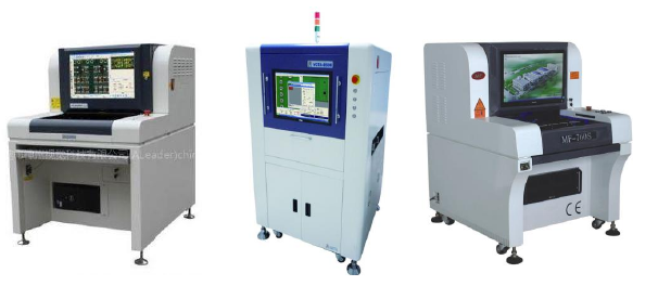
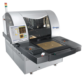
1. 介绍AOI系统的研究背景、意义及国内外的研究现状。通过对PCB检测方法实际生产生活需求的分析,明确检测系统的检测任务和各项性能指标,然后提出自动光学检测系统,表明它在PCB检测中的重要作用,最后论述AOI技术在国内外的研究现状及现在市场上常见的一些AOI设备。
2. 设计AOI检测设备的结构。根据AOI系统的工作原理,分析它的结构组成,并且对现在市场上所用的工业相机镜头等结构部件进行简单的介绍及比较。然后设计出AOI检测设备的运动控制方式,最后根据运动控制方式来设计AOI设备的硬件结构。最后对AOI检测设备的软件结构进行了简单的介绍。
3. 分析比较AOI系统路径规划方法。基于AOI系统的路径规划,有很多种方法。首先最简单的就是基于图像拼接顺序的顺序取像方法,该方法简单易行,但相机拍摄次数较多,最后还要进行图像的拼接处理,增大了后期的图像处理的复杂度,且耗时较长;其次是基于混合遗传算法的路径规划方法,该方法在遗传操作中加入了具有较强局部搜索能力的最近邻搜索算子,就是找到相距最近的视场,然后相机按照顺序依次运动;第三种方法就是一种多阶段路径规划方法,该方法是先初步规划视场位置,然后对路径进行初步规划,根据规划的路径,反向调节视场位置,再根据视场位置找出最短路径。本文是针对工业用相机的单次拍摄窗口大小固定且远小于PCB的板幅面积的特点,提出了一种基于覆盖域的聚类算法,来获取完全覆盖PCB板上所有电子元器件的最少取像窗口集,然后针对相机移动的顺序可自由组合的特点,提出一种遗传算法,利用变异和交叉不停选取最优种群来获得最短的取像路径。最后结合基于混合遗传算法的取像方法、基于图像拼接的顺序取像方法和多路径规划取像等方法,来分析比较各自的特点,最后通过仿真实验,来验证本文提出的方法的可行性及适用性。
关键词:自动光学检测;路径规划;PCB;视场分配
Abstract
In recent years, with the improvement of people's quality of life and informationization level, the requirements for the performance and quality of electronic products are getting higher and higher. As the most important part of electronic products, the quality of printed circuit board (PCB) has become the core issue that the electronic manufacturing industry attaches great importance to. The earliest traditional PCB detection method is manual detection, that is, direct observation of the human body through the naked eye, to detect the defects of PCB board. However, this method can not meet the high-precision and high-speed detection requirements on the production line. Electrical testing and workmanship testing are also phased out because of the high cost of production. Therefore, in order to improve the detection accuracy and speed of PCB, people have developed an automatic optical inspection system (AOI) based on mechanical vision. At the end of the last century, AOI detection technology has been applied and promoted to a certain extent in the world. AOI detection technology started late in China, which affected the research and production of domestic AOI equipment to a certain extent. Therefore, improving the stability of AOI system, reducing the production cost and complexity of the system, optimizing the path planning of AOI system and improving its detection accuracy and speed have become the research focus of automatic optical detection technology.
This paper is mainly based on the automatic optical detection system, in order to achieve high-precision and high-speed detection of PCB, and the path planning of the automatic optical detection system, the specific contents include the following aspects:
1. Introduce the research background, significance and research status of AOI system at home and abroad. Through the analysis of the actual production and living needs of PCB detection methods, the detection tasks and performance indicators of the detection system are defined. Then an automatic optical detection system is proposed, which shows its important role in PCB detection. Finally, the research status of AOI technology at home and abroad and some common AOI equipment on the market are discussed.
2. Design the structure of AOI testing equipment. According to the working principle of AOI system, the structure of AOI system is analyzed, and the industrial camera lens and other structural components used in the market are briefly introduced and compared. Then the motion control mode of AOI detection equipment is designed. Finally, the hardware structure of AOI equipment is designed according to the motion control mode. Finally, the software structure of AOI testing equipment is briefly introduced.
3. Analysis and comparison of AOI system path planning methods. There are many methods for path planning based on AOI system. First of all, the simplest method is the sequential image acquisition method based on image mosaic sequence. This method is simple and feasible, but the number of camera shots is large. Finally, image mosaic processing is needed to increase the complexity of later image processing and take a long time. Secondly, the path planning method based on hybrid genetic algorithm is introduced, which has strong local search in genetic operation. The nearest neighbor search operator of capability is to find the nearest field of view, and then the camera moves in sequence. The third method is a multi-stage path planning method, which is to initially plan the position of the field of view, then make a preliminary planning of the path, adjust the position of the field of view inversely according to the planned path, and then find the shortest path according to the position of the field of view. In this paper, a clustering algorithm based on coverage area is proposed to obtain the minimum set of image-taking windows covering all electronic components on PCB board, aiming at the fixed size of single shot window of industrial cameras, which is much smaller than the plate area of PCB. Then, a genetic algorithm is proposed to solve the problem that the sequence of camera movement can be freely combined. By using mutation and cross-selection, the minimum set of image-taking windows covering all electronic components on PCB board can be obtained. The shortest image acquisition path can be obtained by selecting the optimal population. Finally, combining the methods of image acquisition based on hybrid genetic algorithm, sequential image acquisition based on image mosaic and multi-path planning image acquisition, the characteristics of each method are analyzed and compared. Finally, the feasibility and applicability of the proposed method are verified by simulation experiments.
Key words: automatic optical detection; path planning; PCB; field of view allocation
目录
摘要 I
Abstract III
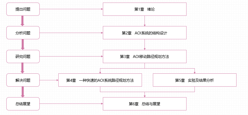
第1章 绪论 1
1.1研究背景与意义 1
1.2国内外研究现状 3
1.3论文的主要内容 6
1.4论文结构 6
第2章 AOI系统的结构设计 8
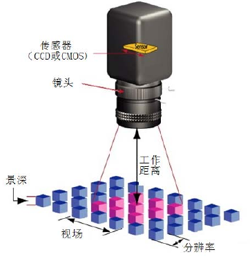
2.1 AOI系统的工作原理 8
2.2 AOI系统硬件结构 8
2.2.1 设备类型 8
2.2.2 硬件系统 10
2.2.3 AOI系统的硬件结构设计 14
2.3 AOI系统的软件结构 18
第3章 AOI移动路径规划方法 19
3.1 基于图像拼接的顺序取像方法 19
3.2 基于混合遗传算法的取像路径规划方法 20
3.3 多阶段的检测路径规划方法 22
第4章 一种快速的AOI系统路径规划方法 27
4.1 基于层次聚类算法的视场分配 27
4.2 基于遗传算法的路径规划 34
4.3 Ui界面设计 37
第5章 实验及结果分析 39
5.1视场分配实验 39
5.2路径规划实验结果 40
5.3小结 42
第6章 总结与展望 44
6.1论文总结 44
6.2工作展望 44
参考文献 46
致谢 48
附录A 视场分配代码 49
附录B 路径规划 60
第1章 绪论
1.1研究背景与意义
近年来,电子产品都在向着轻便、细小、超薄及多功能化和智能化方向发展,印刷电路板产品也向着高精度、高密度、小元件、小间距及超薄型方向快速发展,检测目标的集成度和复杂度越来越高。电子元件的封装尺寸也越来越小,且采用的通路数目越来越少,这对PCB板的加工制造要求也就更高了。
表面贴装技术(Surface Mounted Technology,SMT)是最新的电子组装技术,它可以将体积微小的微型元器件组装在PCB上,目前大多数PCB组装都采用的是这种方式。虽然随着科技不断进步,SMT技术也在不断发展,在是在贴装的过程中,还是会经常引起PCB的一些功能上的缺陷。为了确保每一个元器件都能被放置在正确的位置上,并且按照我们的需求来进行工作,贴装之后就必须要对PCB进行检测。
以上是毕业论文大纲或资料介绍,该课题完整毕业论文、开题报告、任务书、程序设计、图纸设计等资料请添加微信获取,微信号:bysjorg。
相关图片展示: