CuInS2量子点的制备与性能研究毕业论文
2021-12-05 17:30:32
论文总字数:24899字
摘 要
在众多量子点当中,无镉无铅的Ⅰ-Ⅲ-Ⅵ族CuInS2(CIS)三元半导体量子点最引人注目。CuInS2为直接带隙半导体,禁带宽度为1.5 eV,光吸收系数大约为105 cm-1左右,毒性小,在发光器件、太阳能电池和生物医学等领域具有广阔的应用前景。
采用一锅法制备CuInS2量子点,研究反应时间对CuInS2量子点结构、表面形貌和光学性能的影响。利用一锅煮和热注入法相结合的方法制备核壳结构CuInS2/ZnS量子点,研究Cu/Zn摩尔比和反应时间对其结构和性能的影响,探索核壳结构CuInS2/ZnS量子点和CuInS2量子点各自特点。
本文特色在于,通过改变Cu/Zn比研究核壳结构量子点CuInS2/ZnS的发光性能。实验结果表明:
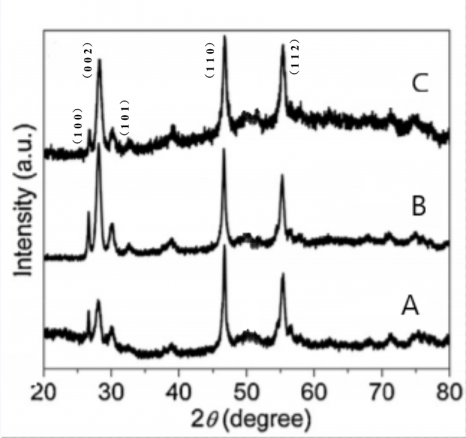
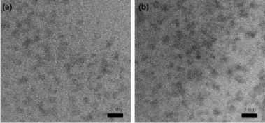
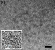
(1)随着反应时间的进行,CuInS2量子点的尺寸不断增大,所得产物的吸收和发射光谱均有不同程度的红移,吸收光谱的肩膀峰由500 nm(反应时间为2 min)移动至541 nm(8 min);PL光谱的发射峰由650 nm(2 min)移动至680 nm(8 min)。所得的CuInS2量子点的荧光发光效率为6%。CuInS2量子点(112)衍射峰的强度随反应时间的增加而变强,颗粒尺寸随着反应时间的延长而增大。TEM图像也表明CuInS2量子点的尺寸随反应时间的延长而增大。
(2)通过研究不同Cu/Zn比对核壳结构量子点的影响发现,与CuInS2量子点比较,随着Cu/Zn比中Zn含量的增加,壳层ZnS含量的增加,核壳结构CuInS2/ZnS量子点的尺寸增大,带隙宽度增加,发射峰从CuInS2量子点的发光峰650-680nm蓝移到620-680nm,光致发光量子产率由CuInS2量子点的6%增加到57%。
(3)核壳结构CuInS2/ZnS量子点随着反应时间的进行,核壳结构的壳层厚度不断增大,所得产物的吸收和发射光谱均有不同程度的红移,如果反应时间过长(>5h),光谱红移现象缓慢且光致发光效率会降低。
关键词:CuInS2量子点;核壳结构量子点;一锅法;热注入法
Abstract
Among those QDs, cadmium-free Ⅰ-Ⅲ-Ⅵ CuInS2 (CIS) ternary semiconductor quantum dots are the most attractive. CuInS2 is a direct band gap semiconductor with a forbidden band width of 1.5 eV, a light absorption coefficient of about 105 cm-1, and low toxicity, which has broad application prospects in light-emitting devices, solar cells, and biomedicine.
A one-pot method was used to prepare CuInS2 quantum dots, and the effect of reaction time on the structure, surface morphology and optical properties of CuInS2 quantum dots was studied. Using a combination of one-pot method and hot-injection method to prepare the core-shell CuInS2/ZnS quantum dots, studying the effect of Cu/Zn molar ratio and reaction time on its structure and performance, exploring the features of core-shell CuInS2/ZnS quantum dots and CuInS2 quantum dot.
The characteristic of this paper is to study the luminescence properties of the core-shell CuInS2/ZnS quantum dots by changing the Cu/Zn ratio. Experimental results show that:
(1) With the progress of the reaction time, the size of CuInS2 quantum dots continues to increase, and the absorption and emission spectra of the resulting products have different degrees of red shift: the shoulder of the absorption spectrum moves from 500 nm (with a reaction time of 2 min) to 541 nm (8 min); the emission peak of the PL spectrum moves from 650 nm (2 min) to 680 nm (8 min). The photoluminescence efficiency of the obtained CuInS2 quantum dots is 6%. Intensity of CuInS2 quantum dot diffraction peak (112) becomes stronger with the increase of the reaction time, and the particle size increases with the extension of the reaction time. TEM also shows that the size of CuInS2 quantum dots increases with the extension of the reaction time.
(2) By studying the effect of different Cu/Zn ratios on the core-shell quantum dots, it is found that compared with CIS, with the increase of the Zn content in the Cu/Zn ratio, the shell ZnS increases, the size of the core-shell CuInS2/ZnS quantum dots and the band gap increase, the emission peak is blue-shifted from 650-680nm of the luminescence peak of CuInS2 quantum dots to 620-680nm, and the photoluminescence quantum yield is increased from 6% of CuInS2 quantum dot to 57%.
(3) With the progress of the reaction time of core-shell CuInS2/ZnS quantum dots, the thickness of the shell layer of the core-shell structure continues to increase, and the absorption and emission spectra of the resulting products have different degrees of red shift. If the reaction time is too long(gt;5h), the spectral red-shift is slow and the photoluminescence efficiency will be reduced.
Key Words:CuInS2 quantum dots, core-shell quantum dots, one-pot method, hot-injection method
目 录
摘 要 I
Abstract II
目 录 IV
第1章 绪论 1
1.1 量子点概述 1
1.1.1 量子点的基本特征 1
1.1.2 量子点的发光原理与光学特性 2
1.1.3 量子点的制备工艺 2
1.2 核壳结构量子点 3
1.2.1 核壳结构量子点概述及分类 3
1.2.2 壳层材料的选择 4
1.3 Ⅰ-Ⅲ-Ⅵ族合金结构量子点 5
1.3.1 Ⅰ-Ⅲ-Ⅵ族合金结构量子点概述 5
1.3.2 CuInS2合金量子点 6
1.3.3 CuInS2/ZnS核壳结构合金量子点 6
1.3.4 CuInS2量子点的制备方法 6
1.4 本论文的研究内容与研究意义 7
第2章 实验部分 8
2.1 实验仪器与试剂 8
2.1.1 实验仪器 8
2.1.1 实验试剂 8
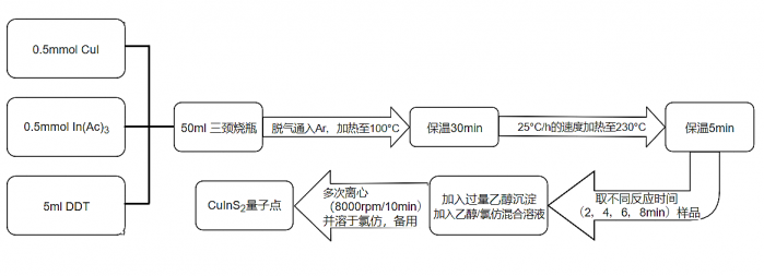
2.2 实验步骤 9
2.2.1 制备CuInS2量子点实验步骤 9
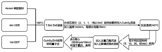
2.2.2 制备CuInS2/ZnS核壳结构量子点实验步骤 9
2.3 表征方法 10
2.3.1 X射线衍射分析(XRD) 10
2.3.2 透射电镜分析(TEM) 10
2.3.3 紫外可见吸收光谱分析(UV-vis) 10
2.3.4 荧光光谱分析(PL) 10
第3章 结果分析与讨论 11
3.1 引言 11
3.2 CuInS2量子点和CuInS2/ZnS核壳结构量子点的制备 11
3.3 CuInS2量子点结果分析与讨论 12
3.3.1反应时间对CuInS2量子点的结构和性能影响 12
3.3.1.1 X射线衍射(XRD)分析 12
3.3.1.2 透射电子显微镜(TEM)分析 13
3.3.1.3 吸收(Absorbance)光谱和光致发光(PL)光谱分析 14
3.4 CuInS2/ZnS核壳结构量子点结果分析与讨论 15
3.4.1 Cu/Zn摩尔比对CuInS2/ZnS核壳结构量子点的结构及性能影响 15
3.4.1.1 X射线衍射(XRD)分析 15
3.4.1.2 透射电子显微镜(TEM)分析 16
3.4.1.3 吸收(Absorbance)光谱和光致发光(PL)光谱分析 16
3.4.2 反应时间对CuInS2/ZnS核壳结构量子点的结构及性能影响 17
3.4.2.1 X射线衍射(XRD)分析 17
3.4.2.2 透射电子显微镜(TEM)分析 18
3.4.2.3 吸收(Absorbance)光谱和光致发光(PL)光谱分析 19
3.5 小结 20
第4章 结论与展望 22
4.1 结论 22
4.2 展望 23
参考文献 24
致 谢 26
第1章 绪论
自20世纪以来,随着煤、石油、天然气等传统能源的日渐匮乏,能源危机已经逐渐成为阻碍人类社会进步与发展的问题之一[1]。与此同时,大量开采和使用传统能源所导致的环境问题温室效应,热岛效应等,已严重影响人们的身体健康与日常生活。因此,开发出无污染的可再生能源材料已迫在眉睫[2]。
在过去的几十年里,量子点材料(Quantum dots, QDs)作为一类新型的无机半导体材料,由于其独特的物理及化学性质而成为研究者们关注的重点[3]。由于量子点拥有可调节的发射波长、较高的光稳定性、较低的成本以及大斯托克斯位移等,在过去的几十年里得到大量的研究与发展[4]。
1.1 量子点概述
量子点作为一种准零维的纳米材料,其在三个维度上的尺寸都小于100 nm[5]。量子点通常由Ⅱ-Ⅵ族或Ⅲ-Ⅵ族元素组成,具有独特的性质[6]。
1.1.1 量子点的基本特征
(1)量子限域效应
当微粒的尺寸很小时,由于空间有限,电子与空穴的运动受到限制,与体材料相比,电子态呈量子化分布,即能级变为离散能级,使其能量变大,发射光谱蓝移,带隙宽度变大,该现象称为量子限域效应。而此程度下的临界尺寸,成为激子波尔半径。
请支付后下载全文,论文总字数:24899字
相关图片展示: